

AT&S investerer stort i udbygning af udviklings- og produktions-faciliteter i Europa
PCB- og mikroelektronikleverandøren AT&S med hovedsæde i Østrig har annonceret en nyinvestering i firmaets Leoben-facilitet på 500 mio. Euro over de næste år (in english).
In view of the ongoing boom in demand in the microelectronics sector and ever-new performance requirements for electronic systems, AT&S has decided to put an even stronger focus on research and development.Therefore, the company is investing in a new R&D center for substrate and packaging solutions for the global semiconductor industry at its location in Leoben-Hinterberg. In addition, another technology upgrade of the production facilities will be implemented. The investments totaling € 500 million are planned up to 2025. The investment total includes previously communicated investments in a technology upgrade and the new AT&S office building.
- Leoben is the central hub of AT&S. Starting here, AT&S has grown to become a global group and today is one of the key players in the high-end printed circuit board and IC substrate business, says Hannes Androsch, Chairman of the AT&S Supervisory Board.
- While we invest heavily in other countries and only recently announced our new location in Kulim/Malaysia, it is exactly these investments in Asia that not only secure our locations and their employees, but also ensure that the site in Leoben is expanded and around 700 highly qualified jobs are being created.
Precursors for IC substrates are already produced in Leoben today and subsequently further processed into high-end final products at the facilities in Chongqing/China and in the future also in Kulim/Malaysia. To meet the growing demand, the production facilities are upgraded and an additional production building of roughly 18,000 m2 will be built.
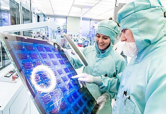
An essential part of the investment will also be used for a new research center including the production of small series and prototypes. With the new, state-of-the-art R&D center, AT&S addresses both customers in the high-end semiconductor segment and international research institutions.
- The technologies used here are unparalleled in Europe and give AT&S a unique selling proposition on the market, says AT&S CEO Andreas Gerstenmayer. Research and development at this level of technology will enable us to offer our customers innovative solutions for future product generations even more proactively and to take on a pioneering role in the industry.
- In addition, this investment is a clear commitment to the location in Leoben and will make a contribution to a competitive microelectronics industry in Europe.
This AT&S project conforms with the European Chip Act, which was announced by Ursula von der Leyen, President of the European Commission, in mid-September. The goal is to jointly create a European state-of-the-art chip ecosystem in order to safeguard security of supply in Europe and to develop new market for European breakthrough technologies.
The investment now announced will also go hand in hand with a significant increase in the number of employees at AT&S. An additional 700 employees will be required by 2025, including engineers in various disciplines, specialists and university graduates for business and technical fields as well as qualified skilled workers.
AT&S is a leading manufacturer of high-end printed circuit boards and IC substrates. AT&S industrialises leading-edge technologies for its core business segments Mobile Devices & Substrates, Automotive, Industrial and Medical.
AT&S has a global presence with production sites in Austria (Leoben, Fehring) and plants in India (Nanjangud), China (Shanghai, Chongqing) and South Korea (Ansan near Seoul). The company employed roughly 10,000 people in the financial year 2019/20. For further information please visit www.ats.net
