

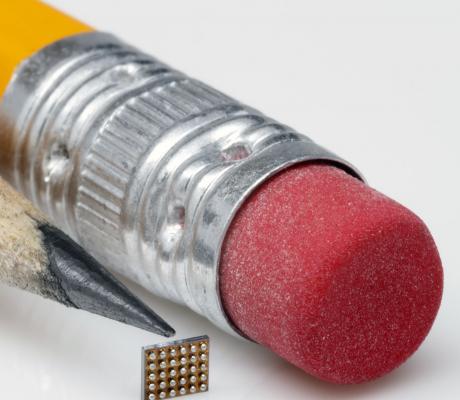
Verdens mindste FPGA med udvidet hukommelse og DSP-faciliteter
De nye iCE40 UltraPlus FPGA-devices fra Lattice Semiconductor åbner for ny innovation inden for bl.a. smartphones og IoT edge-devices (in english).
Lattice Semiconductor has announced its new iCE40 UltraPlus FPGA devices, one of the industry’s most energy-efficient and programmable mobile heterogeneous computing (MHC) solutions. This latest addition to the iCE40 Ultra family delivers eight times more memory (1.1 Mbit RAM), twice the digital signal processors (8x DSPs), and improved I/Os over previous generations.Available in multiple package sizes, the programmable nature of the iCE40 UltraPlus device is ideal for smartphones, wearables, drones, 360 cameras, human-machine interfaces (HMIs) and
industrial automation, as well as security and surveillance products.
Enabling a new way to interact with electronic devices, the iCE40 UltraPlus device is well suited
for voice recognition, gesture recognition, image recognition, haptics, graphics acceleration,
signal aggregation, I3C bridging and more. This brings added intelligence to smartphones and
IoT edge products, such as wearables and home audio assisted devices, to be always on,
always listening and ready to instantly process commands locally without going to the cloud.
The MHC paradigm is concentrated around a highly energy-efficient method for computing
algorithms quickly and locally using dissimilar processors to offload power hungry application
processors (APs) in battery-powered devices. More DSPs offer the ability to compute higherquality algorithms, while increased memory allows data to be buffered for longer low-power states. The flexible I/Os enable a more distributed heterogeneous processing architecture.
This combination provides flexibility to enable OEMs and the Maker market to quickly deliver key innovations, such as always on sensor buffers and acoustic beam forming. Imagine interacting with your mobile product, but without ever touching it. The iCE40 UltraPlus
device will enable the responsiveness required to deliver this functionality. Applications include,
but are not limited to:
• Always-on sensor buffer & distributed processing for mobile devices at sub-1 mW power
consumption
o Always-on sensor functionality while the AP is in sleep mode
o Enables functions such as gesture detection, facial recognition, audio
enhancement, audio beam forming, phrase detection, double tap, shake-to-wake
and pedestrian dead reckoning (PDR)
• Frame buffer and graphics acceleration for wearables and white goods
o Always-on display while AP is in sleep mode
o Interface bridge from MCU to display
o Multi-layer graphics acceleration for improved system power consumption
• Microphone array beamforming for battery-powered mobile devices
o Superior audio quality using multiple mics for background noise reduction as well as audio equalization
• Aggregating various GPIOs, SPI, UART, I2C, I3C signals and more over a single PCB
trace eliminates routing contention issues to reduce system cost and simplify designs
- Distributed processing demands are increasing in mobile applications and Lattice’s iCE40
UltraPlus is optimized to address these requirements. As the newest addition to our
successful iCE40 Ultra product family, the iCE40 UltraPlus FPGAs expand its market reach
to system designers who require FPGA functionality with improved DSP compute power, more
I/Os and increased memory for buffering. Our solution will reduce design complexity, system power consumption and time-to-market, while enhancing responsiveness of tomorrow’s mobile devices, says C.H. Chee, senior director of marketing, mobile & consumer division at Lattice Semiconductor.
Key features of the iCE40 UltraPlus product include:
• Integrated 1.1 Mb SRAM, 8 DSP blocks, up to 5K LUTs and Non-Volatile Configuration
Memory (NVCM) for instant-on applications
• MIPI-I
3C support for low-resolution, always-on camera applications
• Sub 100 micro watt of standby power consumption
• Compact form factor with package sizes starting as low as 2.15 x 2.55 mm for spaceconstrained
consumer markets
• QFN package suitable for addressing industrial market needs
• Ideal for critical low-latency acceleration functions
The iCE40 UltraPlus product evaluation samples and boards are now available.
http://www.latticesemi.com/iCE40UltraFamily.
