

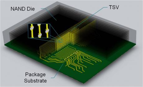
NAND flash med 16 'stakkede' dies
Toshiba udvikler verdens første 'stakkede' 16-die NAND flash hukommelse ved brug af TSV-teknologi (in english).
Toshiba Corporation has announced the development of the world’s first 16-die (max.) stacked NAND flash memory utilising Through Silicon Via (TSV) technology. The prototype will be shown at Flash Memory Summit 2015, to be held from August 11 to 13 in Santa Clara, USA.The prior art of stacked NAND flash memories are connected together with wire bonding in a package. TSV technology instead utilises the vertical electrodes and vias to pass through the silicon dies for the connection. This enables high-speed data input and output, and reduces power consumption.
Toshiba’s TSV technology achieves an I/O data rate of over 1Gbps which is higher than any other NAND flash memories with a low voltage supply: 1.8V to the core circuits and 1.2V to the I/O circuits and approximately 50%2] power reduction of write operations, read operations, and I/O data transfers.
This new NAND flash memory provides the ideal solution for low latency, high bandwidth and high IOPS/Watt in flash storage applications, including high-end enterprise SSD.
A part of this applied technology was developed by the New Energy and Industrial Technology Development Organization (NEDO).
