

Industriens mindste embedded NAND Flash hukommelser
Toshiba's nye såkaldte e∙MMC hukommelser benytter de seneste 15nm NAND Flash hukommelser (in english).
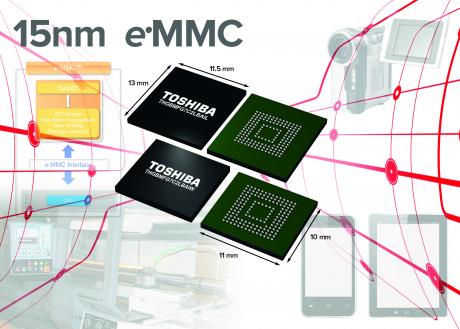
Toshiba Electronics Europe has launched the world’s smallest-class of embedded NAND flash memory products integrating NAND chips fabricated with cutting-edge 15nm process technology. The new memory devices are compliant with the latest e∙MMC standard, and are designed for a wide range of applications including smartphones, tablet PCs and wearable devices. Sample shipment of the 16GB devices start from today, with 8GB, 32GB, 64GB and 128GB products to follow.The e∙MMC NAND chips are fabricated using Toshiba's cutting-edge 15nm process technology and the devices integrate a controller that manages basic control functions for NAND applications. By utilizing the 15nm NAND chips, the package size is approximately 26% smaller[3] than comparable Toshiba products[4]. The153-ball FBGA packages are suitable for use in smartphones, tablet PCs and wearable devices where miniaturization and weight savings are key requirements.
The 16GB e∙MMC NAND chips are available in several package sizes, 11.5 x 13.0 x 0.8mm (THGBMFG7C2LBAIL), 11.0 x 10.0 x 1.0 mm (THGBMFG7C2LBAIW) and 11.5 x 13.0 x 0.8 mm (THGBMFG7C1LBAIL). The 8GB, 32GB and 64GB devices are also available in the 11.5 x 14.0 mm and 11.0 x 10.0 mm formats.
Embedded in a system, the 128GB device (THGBMFT0CBLBAIS) measures 11.5 x 13.0 x 1.4 mm and can record up to 16.3 hours of full spec high definition video and 39.7 hours of standard definition video.
The devices also offer faster read/write performance due to improvements in basic chip performance and controller optimization. The read speed is approximately 8% faster (max.), while the write speed is approximately 20% faster (max.).
Demand continues to grow for NAND flash memory that can support applications such as smartphones and tablet PCs. This is particularly true for embedded memories with a controller, which minimize development requirements and ease integration into system designs. Fully compatible with the latest JEDEC standards, the e∙MMC device interface handles essential functions, including writing block management, error correction and driver software.
The integrated chip design simplifies system development, allowing manufacturers to minimize development costs and speed up time to market for new and upgraded products. Additional new features[6] such as BKOPS control, Cache Barrier, Cache Flushing Report, and Large RPMB Write, have been implemented to further enhance usability. The operating temperature range of -25C to +85C ensures the devices can be specified for use in a wide range of environments and applications.
